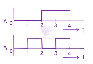
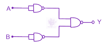
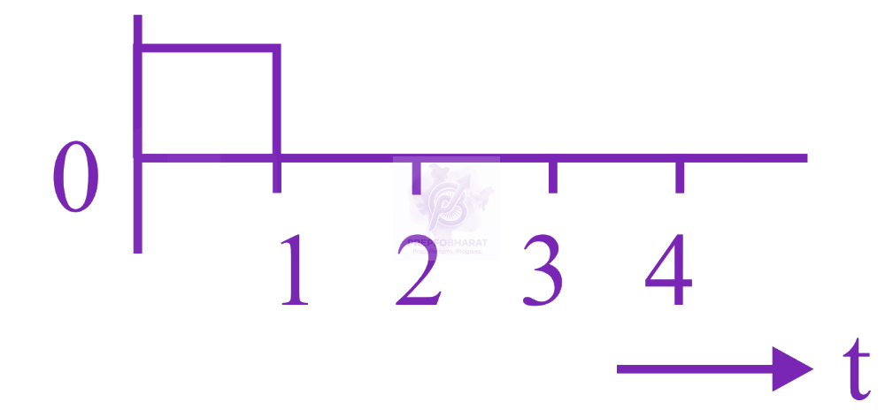
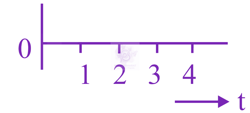
All the gates used in the diagram represent NAND gates.
Thus, the output Y can be calculated as follows
Y===A⋅BA+BA+B
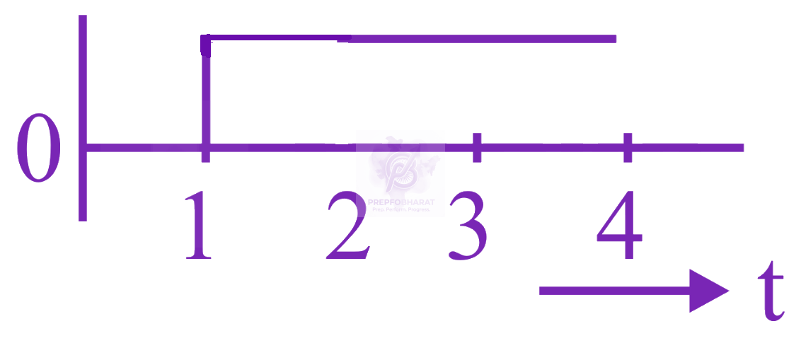
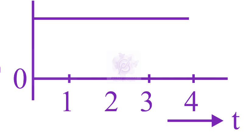
The above equation suggests that the output of the given combination yields the same result as an OR gate.
The truth table can be written as follows
| A | B | A | B | Y=A⋅B |
| 0 | 0 | 1 | 1 | 0 |
| 0 | 1 | 1 | 0 | 1 |
| 1 | 0 | 0 | 1 | 1 |
| 1 | 1 | 0 | 0 | 1 |